AES-128 on an iCE40 FPGA
aes
For the second hardware security task, I implemented AES-128 on a Lattice iCE40-HX8K FPGA. The board receives one plaintext block over UART, encrypts it in hardware, and sends the ciphertext back to the host.
I already knew AES from the software side, where a function accepts a key and a block and returns a ciphertext. The FPGA removed that abstraction. The same operation became registers, lookup tables, byte permutations, finite-field arithmetic, a key schedule, and a controller that had to apply every step exactly once.
The equations were not where I spent most of the effort. I had to decide how bytes were ordered, which state owned each round operation, and when the block cipher had actually "finished." Toolchain behaviour also mattered, since a correct design is not useful if the simulation path is broken.
What the task does
The final design accepts one 128-bit plaintext block through the UART interface provided by the lab framework. The AES core encrypts the block with a fixed 128-bit key from the NIST FIPS-197 example, and the wrapper sends the 128-bit ciphertext back over the same serial link.
I kept the UART wrapper separate from the cipher core. The wrapper is responsible for collecting 16 bytes, starting encryption, waiting for the result, and sending 16 bytes back. The AES core only sees a complete plaintext block, a complete key, and a start/reset-style control signal.
WAIT_FOR_PLAIN -> ENCRYPT -> SEND_CIPHERI made that separation so I could test the AES datapath as a block-level design in cocotb before involving serial timing. Once those tests passed, UART was only a transport layer around an already verified cipher core.
The full system looks roughly like this:
PC
  |
  | UART plaintext, 16 bytes
  v
top_level.v
  |
  +-- uart.v
  |
  +-- aes_module.v
        |
        +-- aes.v
              |
              +-- subbytes.v
              |     +-- sbox.v
              |
              +-- shiftrows.v
              |
              +-- mixcolumns.v
              |     +-- xtime.v
              |
              +-- keysched.v
                    +-- sbox.v
                    +-- rcon.v
Why AES worked as an FPGA exercise
AES is small enough to fit into a lab assignment, but it still forces real hardware trade-offs. The sixteen byte substitutions can be done with sixteen S-boxes in parallel, or one S-box can be reused over several cycles. The key schedule can run alongside the datapath or be precomputed. The round operations can be grouped into larger combinational blocks or split across more registers.
I used a direct implementation. It is not the smallest possible AES core, but it is readable. The structure follows the standard closely, and that made debugging easier. The cost is visible in the final FPGA report: sixteen S-box lookups and a direct round datapath are not free just because the source code looks compact.
This implementation stopped AES from being a black box for me. Each operation became a hardware block with explicit timing, resource, and byte-order contracts.
The AES round structure
AES always encrypts 128-bit blocks. This task used AES-128, so the key is also 128 bits and the cipher runs for ten rounds.
initial round:  AddRoundKey

rounds 1..9:    SubBytes
                ShiftRows
                MixColumns
                AddRoundKey

round 10:       SubBytes
                ShiftRows
                AddRoundKey
The final round intentionally skips MixColumns. That rule is
easy to remember while reading the standard, but a round counter and FSM
can still apply it at the wrong time.
In the integrated core, I already knew what each AES operation did. The open questions were which round key belonged to the current state, when the counter should advance, and whether an extra FSM cycle could apply an operation twice.
The AES FSM ended up following this structure:
IDLE
  initial AddRoundKey

for rounds 1..9:
  SUB_BYTES
  SHIFT_ROWS
  MIX_COLUMNS
  KEY_SCHED
  KEY_ADD

round 10:
  SUB_BYTES
  SHIFT_ROWS
  KEY_SCHED
  KEY_ADD
  DONE
The NIST vector and the byte-order contract
The reference test vector came from NIST FIPS-197. The plaintext, key, and expected ciphertext are:
plaintext:   3243f6a8885a308d313198a2e0370734
key:         2b7e151628aed2a6abf7158809cf4f3c
ciphertext:  3925841d02dc09fbdc118597196a0b32
These values are extremely useful, but only if the implementation agrees on how bytes are packed into the internal 128-bit state. In the wrapper, bytes arriving from UART are placed into the register with:
aes_din[bytecount*8 +: 8] <= uart_data_from_rx;That means the first received byte goes into the least significant byte of the 128-bit register. The fixed key in the Verilog wrapper is therefore stored in reversed byte order:
.keyin(128'h3c4fcf098815f7aba6d2ae2816157e2b)This looks strange until the whole path is written down. The key is the NIST key, but arranged to match the local register convention. Once the convention is fixed, every module has to respect it: UART packing, the AES state layout, the key schedule, the Python reference model, and the final board-level checker.
Byte-order bugs are difficult to spot because the circuit still produces 128 bits and the waveform can look reasonable. Those 128 bits are simply wrong, with no crash to point at the cause. I therefore used the exact test vector as the deciding check.
The state layout was the first real trap
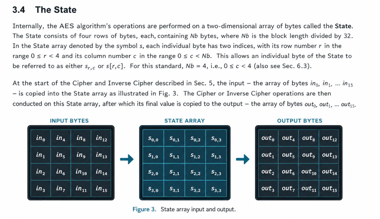
AES describes its internal state as a 4x4 byte matrix. The slightly unintuitive part is that input bytes fill the matrix column-wise:
byte0   byte4   byte8    byte12
byte1   byte5   byte9    byte13
byte2   byte6   byte10   byte14
byte3   byte7   byte11   byte15
Inside the Verilog modules, byte i is selected with
state[8*i +: 8]. That convention made local module code
simple, but it also meant that the "visual" matrix and the packed
register were always one mental translation apart.
This mattered most in ShiftRows and the key schedule.
A row-major mental model combined with a column-major implementation
gives perfectly valid Verilog and invalid AES.
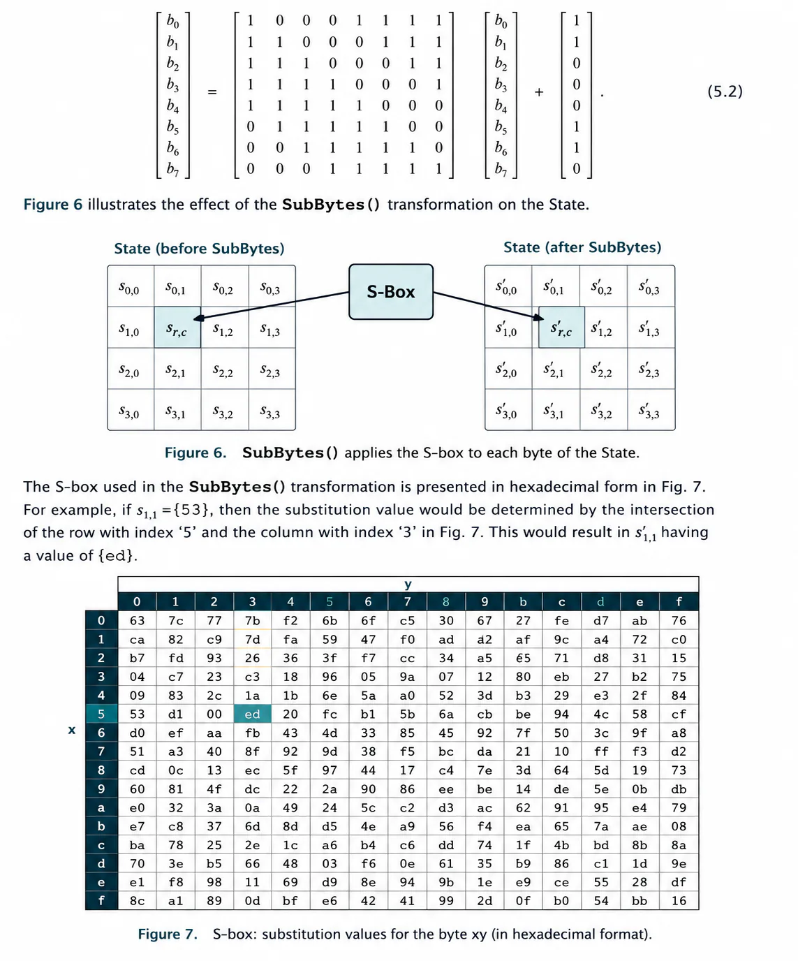
SubBytes: sixteen lookup tables
SubBytes applies the AES S-box independently to every byte.
The S-box itself comes from a multiplicative inverse in
GF(2^8) followed by an affine transformation. The hardware
does not recompute that derivation. It uses the resulting 256-entry
mapping directly.
I instantiated one S-box per state byte, so all sixteen substitutions happen in parallel:
for each byte i:
  state_out[i] = sbox(state_in[i])
I chose this direct version because it was easy to inspect and test. It spends area, so sixteen parallel S-boxes were a real design decision on the small iCE40 FPGA.
ShiftRows: just wiring, until the wiring is wrong
ShiftRows contains no arithmetic. Row zero is unchanged,
row one is shifted by one byte, row two by two bytes, and row three by
three bytes.
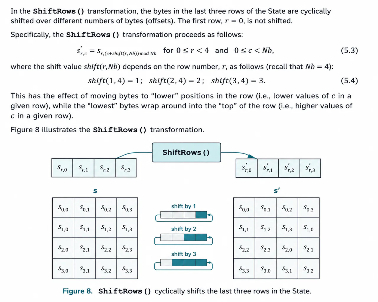
This looked like the easiest module, so I used it to test whether I had understood the state representation. There is no arithmetic to hide a mapping mistake here. If one byte moves to the wrong position, the whole cipher is wrong.
MixColumns: finite-field arithmetic shows up
MixColumns operates on one four-byte state column at a time.
Each column is multiplied by a fixed matrix over GF(2^8).
Addition in this field is XOR. Multiplication is polynomial
multiplication reduced by the AES irreducible polynomial:
m(x) = x^8 + x^4 + x^3 + x + 1
The useful primitive is xtime, which multiplies a byte by
02. In hardware, this becomes a left shift plus a
conditional XOR with 0x1b when the original high bit was
set.
mul2(x) = xtime(x)
mul3(x) = xtime(x) ^ x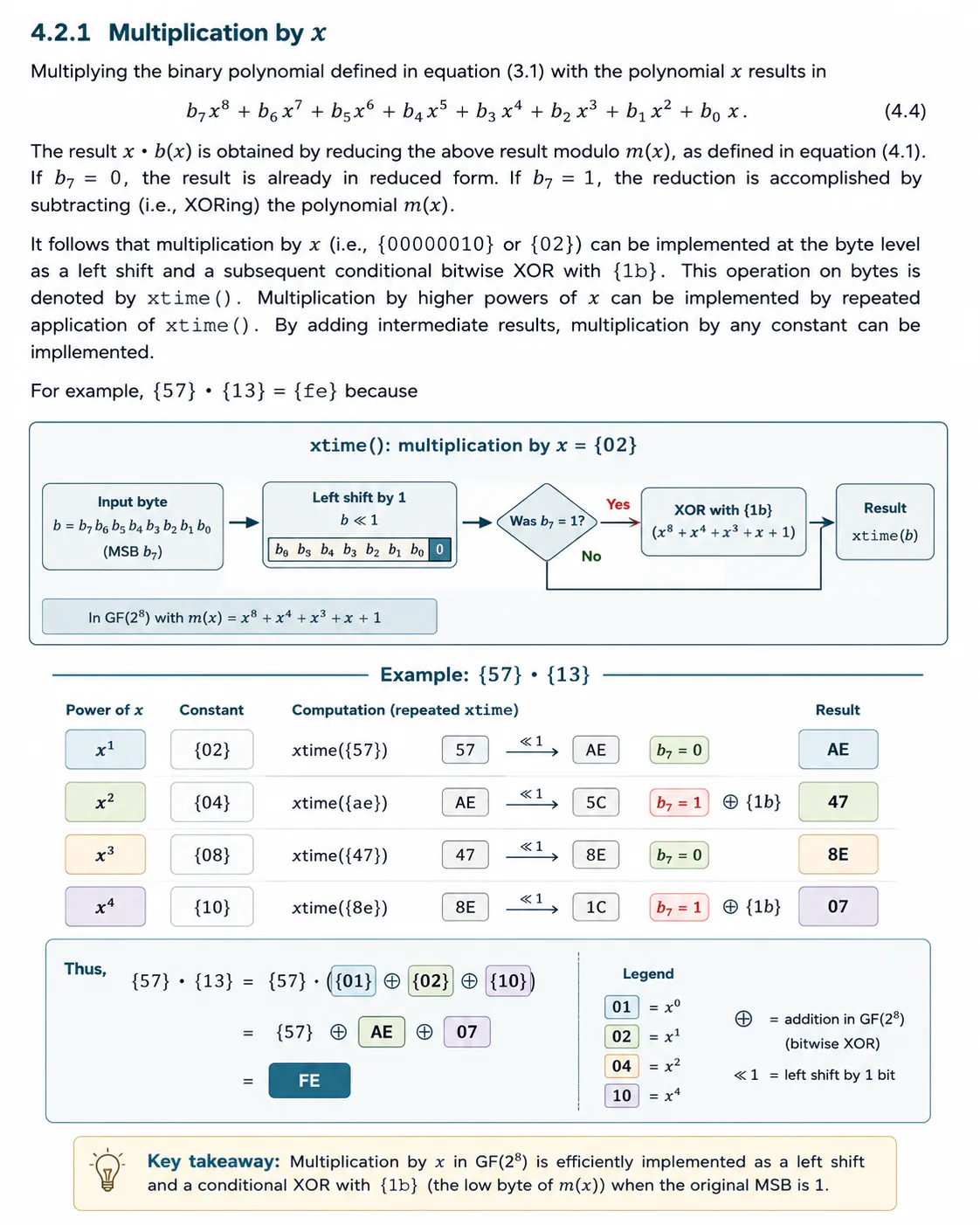
For a column [b0, b1, b2, b3], the forward AES
transformation is:
out0 = 02*b0 ^ 03*b1 ^ 01*b2 ^ 01*b3
out1 = 01*b0 ^ 02*b1 ^ 03*b2 ^ 01*b3
out2 = 01*b0 ^ 01*b1 ^ 02*b2 ^ 03*b3
out3 = 03*b0 ^ 01*b1 ^ 01*b2 ^ 02*b3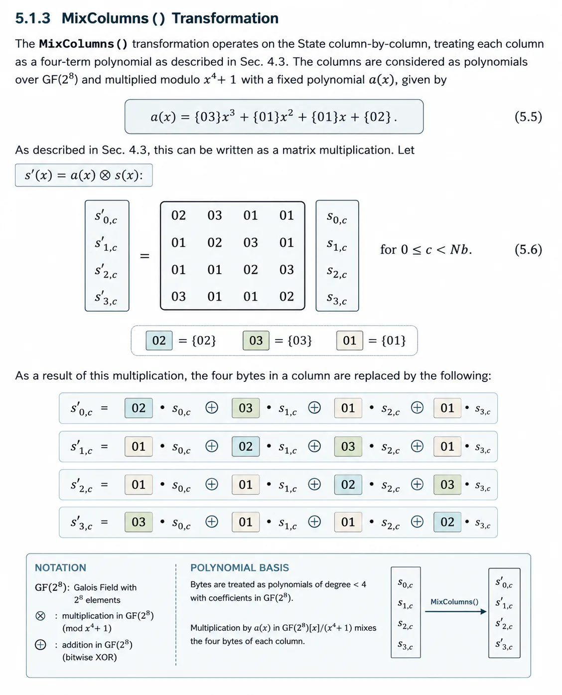
The equations are compact, but the datapath made their cost visible. Every multiply-by-two and multiply-by-three became gates and XOR paths.
AddRoundKey and the danger of simple operations
AddRoundKey is mathematically simple: XOR the 128-bit state
with the current 128-bit round key.
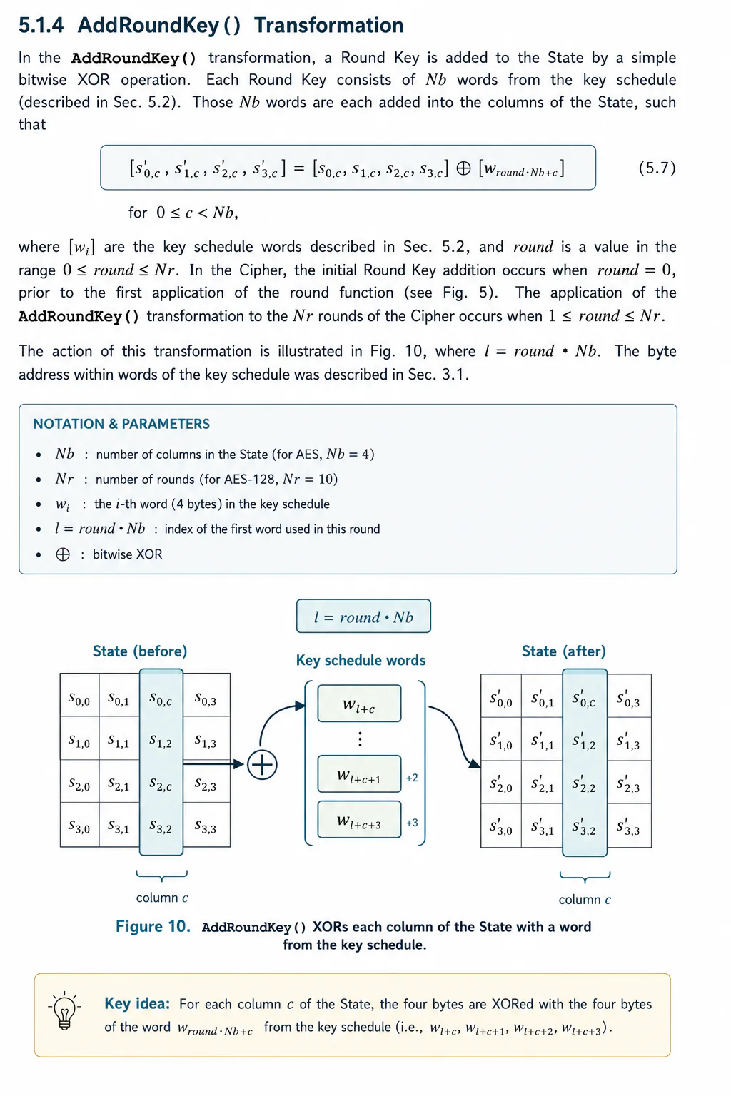
In the controller, simple operations are still dangerous. XORing the same key twice removes it again. If the FSM accidentally remains in the key-add state for an extra cycle, a correct transformation can quietly undo itself.
I therefore gave AddRoundKey clear state ownership: enter the state, apply the key once, then advance. Without that rule, a valid operation could quietly undo itself in sequential hardware.
The key schedule is part of the datapath
AES-128 expands the original 128-bit cipher key into eleven 128-bit round keys: one for the initial AddRoundKey and one for each of the ten AES rounds.
K = w0 || w1 || w2 || w3
To generate the next key, the last word of the previous key goes through
RotWord, SubWord, and an XOR with
Rcon. The remaining words are generated through chained
XORs:
RotWord([a0, a1, a2, a3]) = [a1, a2, a3, a0]
SubWord(word)             = apply S-box to each byte
Rcon[i]                   = [x^(i-1), 00, 00, 00] in GF(2^8)

temp = SubWord(RotWord(w3)) ^ Rcon[round]

nw0 = w0 ^ temp
nw1 = w1 ^ nw0
nw2 = w2 ^ nw1
nw3 = w3 ^ nw2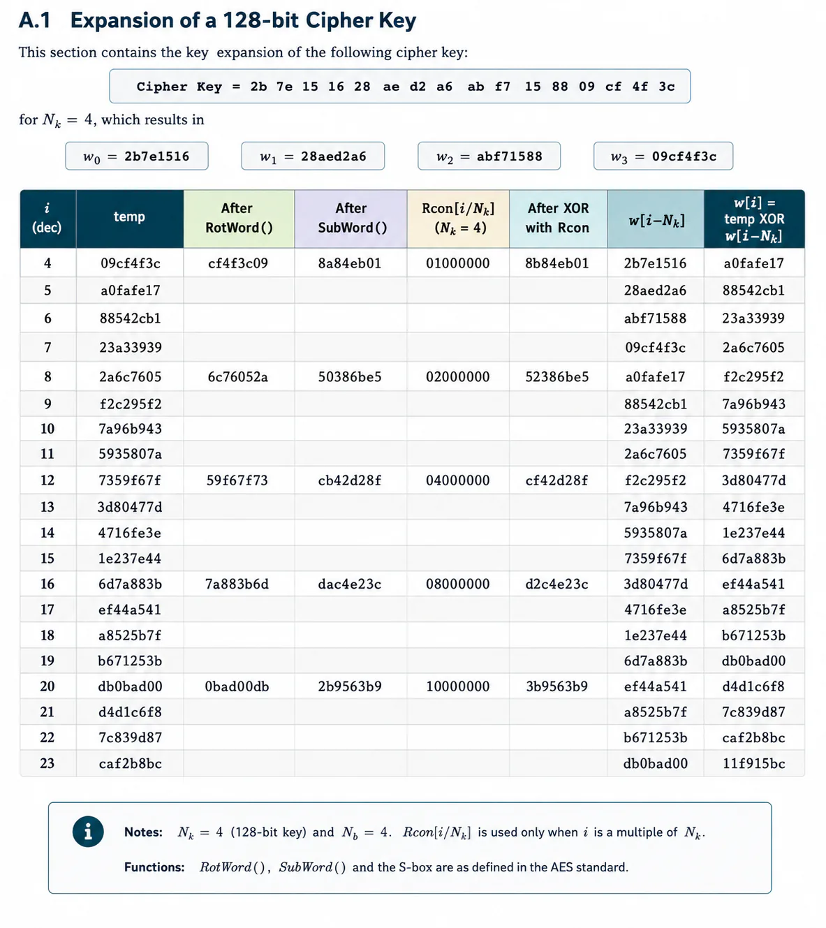
I initially treated key expansion as a helper around the cipher. That model failed once I integrated the controller. The key schedule is part of the datapath synchronization problem, since correct round operations still produce a wrong ciphertext with an off-by-one round key.
Once I fixed the byte order, I verified this module independently. Each generated word follows from the previous word, so the testbench could catch schedule mistakes without running the whole cipher.
Toolchain debugging is still debugging
Much of the work happened outside the AES equations. I first had to make sure the tools were observing the design I thought they were observing.
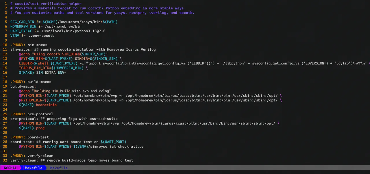
The project used cocotb, Icarus Verilog, vvp, and a Python
AES reference package. On macOS, mixing the oss-cad-suite
vvp binary with a Homebrew Python environment led to
confusing Python embedding errors. The clean solution was to separate
the flows:
simulation:
  Homebrew Icarus Verilog + Homebrew Python venv

FPGA build/programming:
  oss-cad-suite yosys, nextpnr, icetime, icepack, iceprog
This failure was in the simulation path, not the circuit. Separating the two flows let me distinguish a design bug from a broken way of observing the design.
Verification
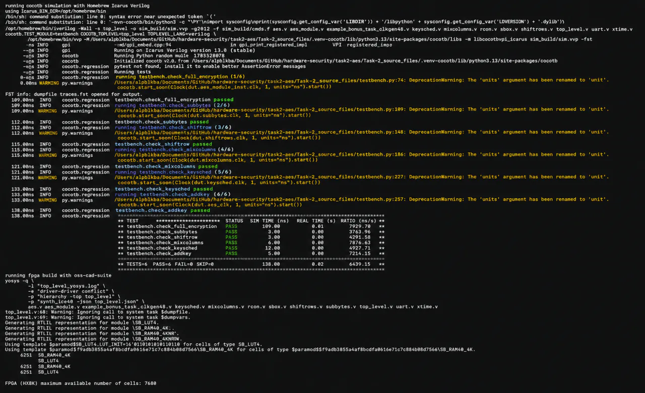
I verified each transformation before trusting the integrated AES core. This let me isolate a wrong ciphertext without reopening every equation from the beginning.
check_full_encryption   PASS
check_subbytes          PASS
check_shiftrow          PASS
check_mixcolumns        PASS
check_keysched          PASS
check_addkey            PASS

TESTS=6 PASS=6 FAIL=0 SKIP=0
The full encryption test uses the NIST FIPS-197 vector. The submodule tests made it possible to isolate bugs in the S-box mapping, row permutation, finite-field arithmetic, key schedule, or AddRoundKey logic before blaming the whole core.
FPGA result
The final design was synthesized and placed with the open-source iCE40 flow: Yosys, nextpnr-ice40, icetime, icepack, and iceprog.
target:        Lattice iCE40-HX8K, ct256
logic cells:   6390 / 7680 = 83%
block RAMs:    4
nextpnr fmax:  104.58 MHz
icetime fmax:  97.64 MHz
target clock:  12 MHz
At 83% logic utilization, this is not a tiny AES core. The direct structure and parallel S-boxes trade area for readability and a simple control structure. For this task, that was the right trade-off: the design still fits on the HX8K and comfortably meets the 12 MHz target used by the UART-based lab setup.
A smaller implementation could reuse fewer S-boxes across multiple cycles. A faster one could pipeline the round logic more aggressively. This version prioritizes a transparent mapping from the standard to hardware.
Board-level test
For the final check, I programmed the FPGA, sent the NIST plaintext over UART, and read the ciphertext back from the board.
Using UART device: /dev/cu.usbserial-21401
Sending plaintext...
Received ciphertext: 3925841d02dc09fbdc118597196a0b32
Correct ciphertext:  3925841d02dc09fbdc118597196a0b32
AES seems to be working correctly, congratulations!
Finished
The design passed module-level simulation, full encryption simulation, FPGA implementation, timing, bitstream generation, and the real UART path on hardware.
Where the implementation was fragile
I knew that AES contained SubBytes, ShiftRows, MixColumns, AddRoundKey, and a key schedule before writing the Verilog. I did not yet know how much state ownership and byte ordering sat behind those names.
Byte order became a contract between every layer of the project. The key schedule needed just as much attention as the visible round operations. A 128-bit XOR had to be protected from being applied twice. The simulator and synthesis tools needed a stable workflow before their output could be trusted.
The final design depended on the datapath, FSM, UART wrapper, Python reference model, FPGA, and toolchain agreeing on those contracts. A mismatch in any one of them was enough to return the wrong ciphertext.