SRAM Weak PUF Readout on iCE40
puf
I read an SRAM PUF response from a Lattice iCE40 board for the first task in a hardware security course. I expected to spend most of the time on security, but the work went into proving that the response was real. Before I could discuss any security property, I had to make sure every byte left the FPGA and reached the PC without the measurement pipeline inventing an artifact.
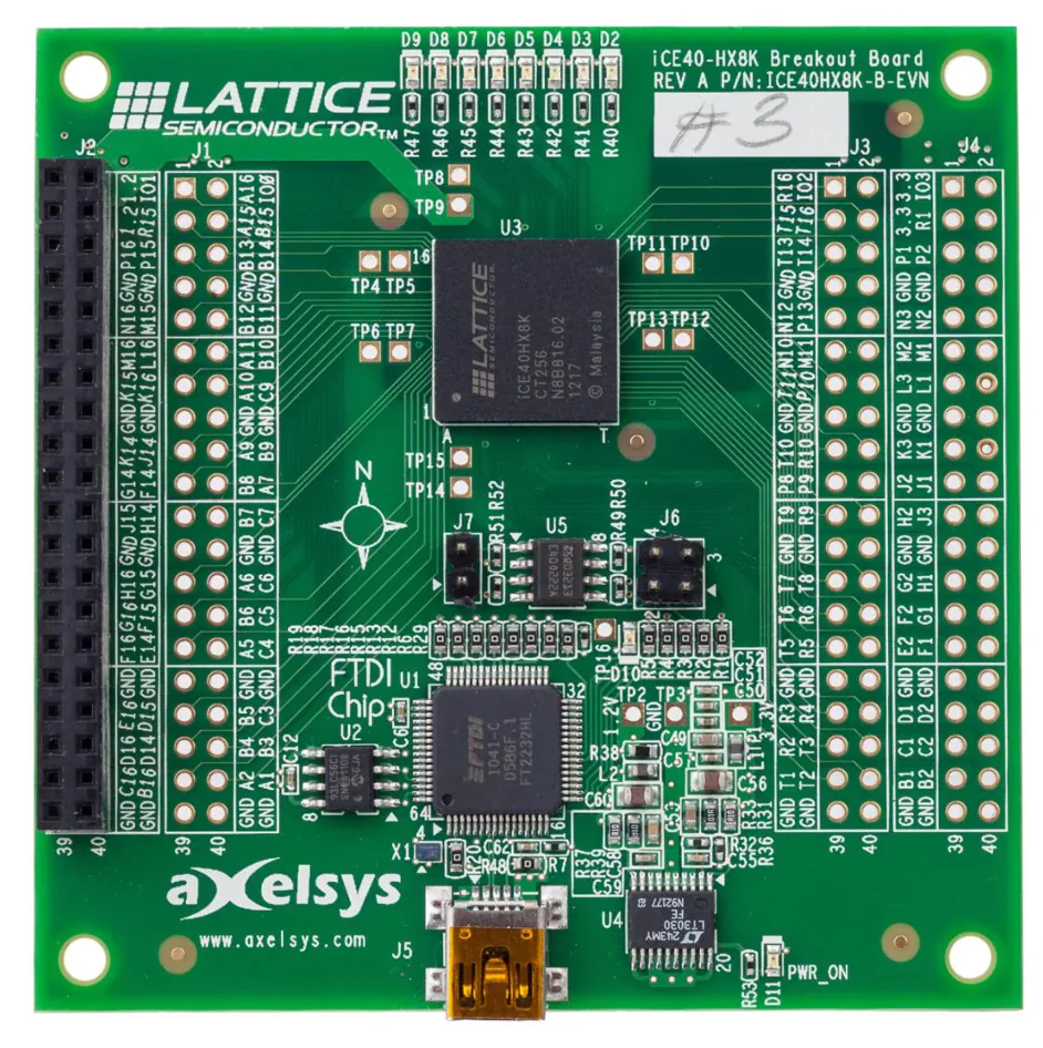
A physical unclonable function, or PUF, derives a device-specific response from manufacturing variations already present inside the chip. The value comes from the physical device rather than non-volatile memory that stores a fixed secret.
Two chips made from the same design still differ slightly at the physical level. A PUF tries to turn those differences into a reproducible digital fingerprint.
What a weak PUF is
A weak PUF exposes one or a small number of challenge-response pairs. This makes it useful as a device fingerprint: power up the device, read the response, and use it to identify or characterize that physical instance.
A strong PUF instead supports a large challenge-response space. I was not building an authentication protocol in this task. I first needed to learn whether I could read a hardware-derived startup pattern reliably, then analyse whether it behaved like a useful fingerprint.
Why SRAM
SRAM cells are built from cross-coupled inverters. Ideally, an uninitialized cell could power up as either 0 or 1. In real silicon, tiny mismatches between transistors make some cells slightly prefer one state over the other.
A cell that tends to power up to the same value across repeated cycles can contribute to a device-specific response. A cell that changes randomly is less useful for identification, although it still describes the physical behaviour of the memory.
SRAM, BRAM, and the FPGA detail
In a microcontroller or processor, SRAM usually means general on-chip static memory. On an FPGA, the name can be confusing because the fabric exposes embedded block memories, or BRAMs.
The naming difference did not affect the measurement. What mattered was that the memory had a power-up state before the design intentionally overwrote it. The readout circuit had to capture that state and stream it to the host before I treated the data as a PUF response.
What this task does
The implementation reads startup memory on a Lattice iCE40 FPGA, sends the raw response to a PC over UART, and analyses data collected across repeated power cycles.
The analysis covers the usual first-order PUF metrics: uniformity, bit-aliasing, uniqueness, and reliability. Those metrics only mean something if the readout path is trustworthy. A broken UART transfer or an off-by-one address bug can look like a bad PUF even when the physical source behaves correctly.
During bring-up, I recorded each UART and FSM failure beside the PUF measurement it affected. That made the boundary clear: the startup value came from the memory, while the address logic and transport decided whether I ever observed that value correctly.
Setup
The task collected SRAM startup data from the FPGA and sent it to the host. The circuit was small, but the measurement crossed state transitions, counters, UART handshakes, and host-side validation.
Build workflow
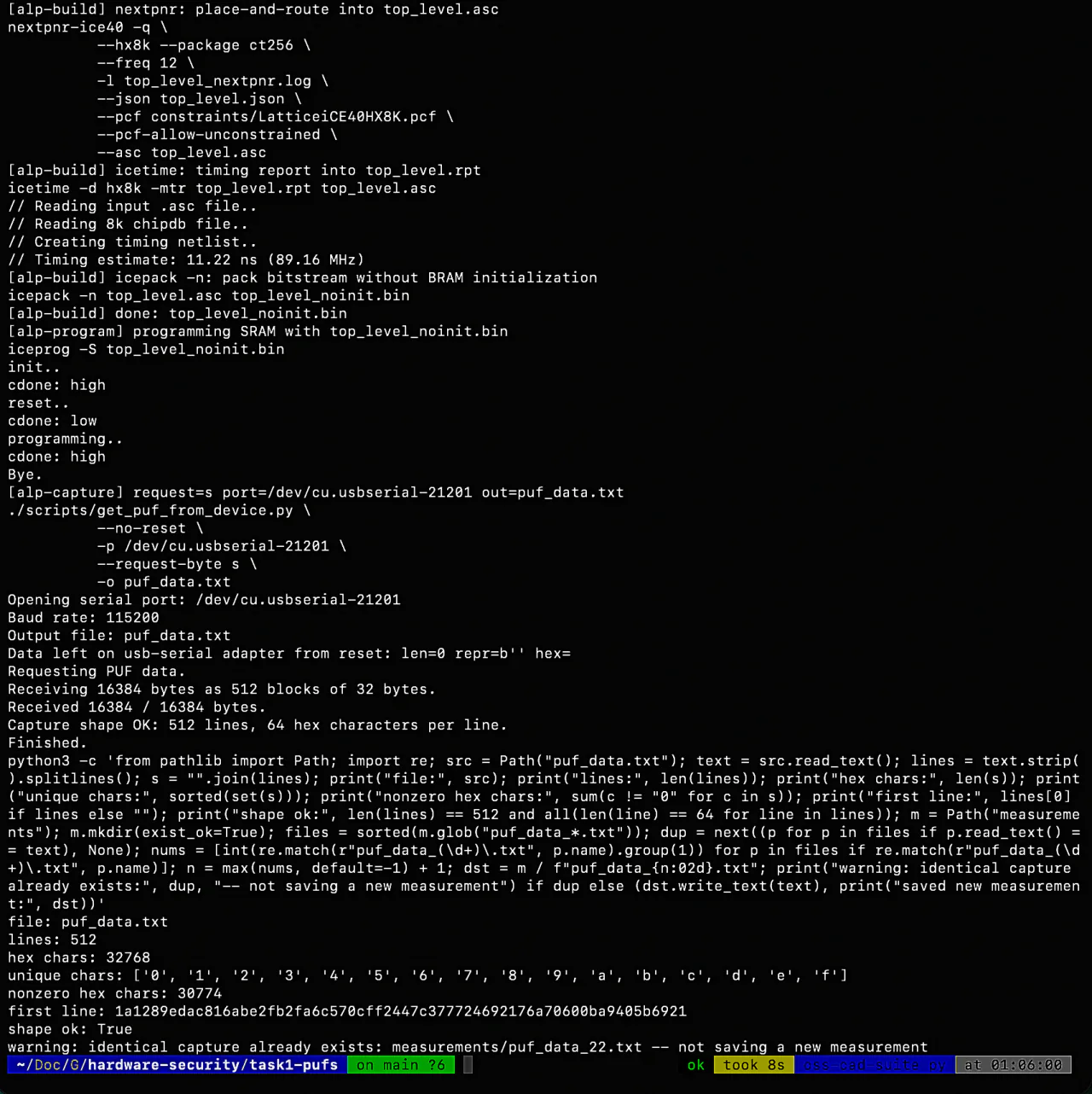
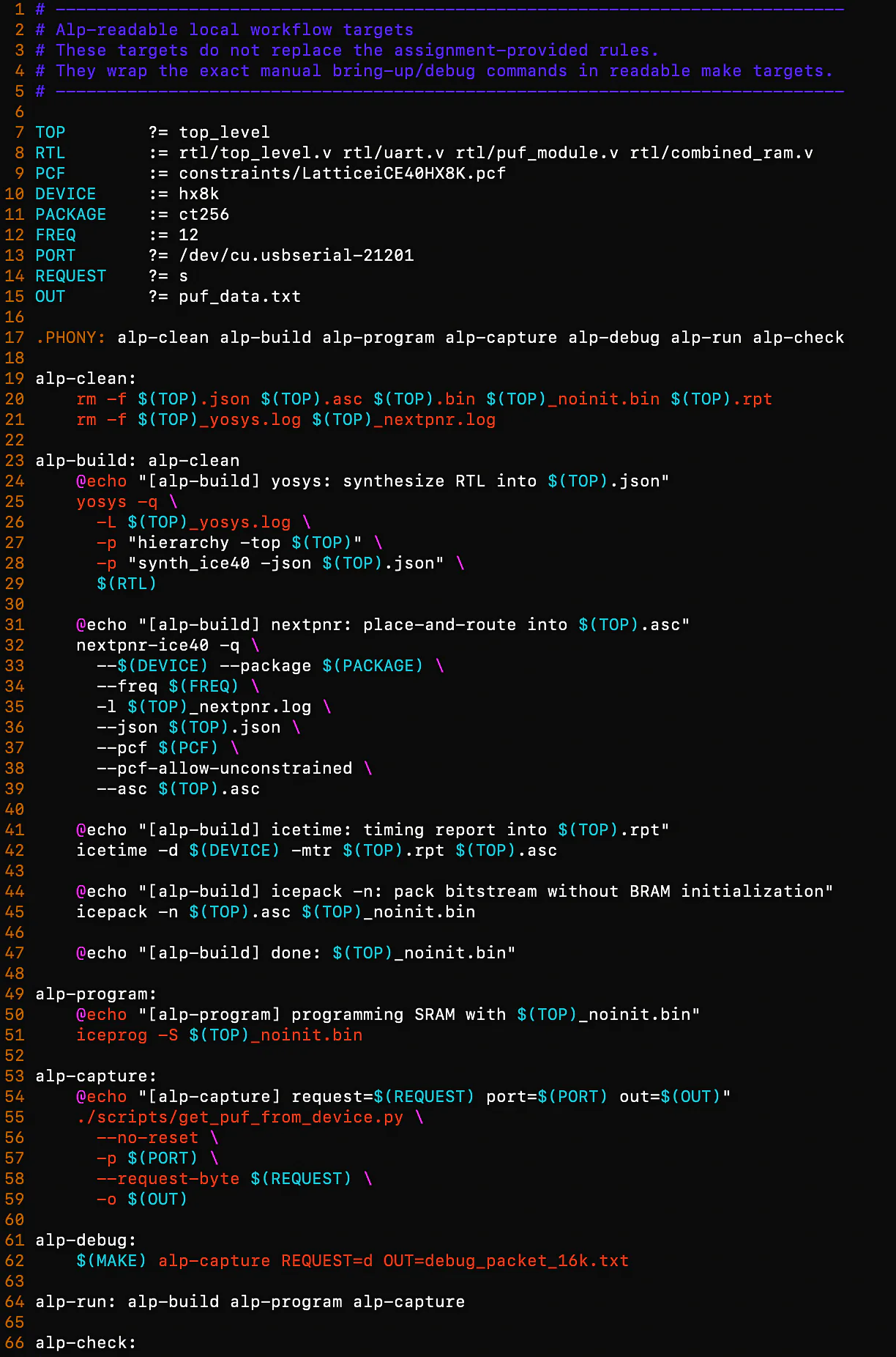
Before taking measurements, I made the design build, flash, and run in a repeatable way. I initially treated the process as "compile the Verilog and flash the bitstream." After repeating the same Yosys, nextpnr, icepack, and programmer commands, I moved them into a small Makefile to avoid copy-paste mistakes while debugging.
Trusting the measurement
Turning the FPGA into a measurement instrument took more work than the PUF concept itself. Until I verified the readout path, every PUF metric remained suspect.
Before analysing uniqueness, stability, entropy, or security properties, I had to answer a narrower question: was I receiving the bytes that the FPGA intended to send?
The data path crossed FPGA memory, read address generation, byte selection, UART transmission, host-side capture, and Python analysis. I checked each boundary before using the final data.
Readout pipeline
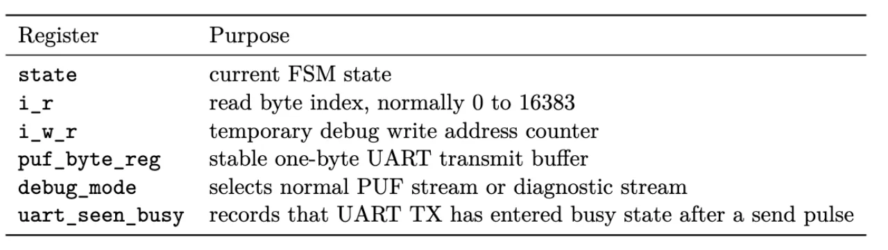
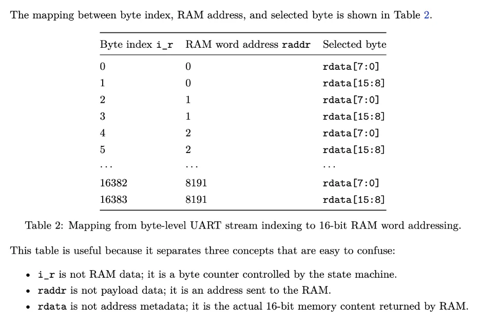
The design follows a small FSM. It waits for a command from the host, decides whether this is a normal PUF readout or a diagnostic request, reads memory words, selects the correct byte, hands that byte to the UART transmitter, waits until the transmitter really finished, and then moves to the next byte.
The PC only sees a serial byte stream. The FPGA has to maintain the current byte index, derive the RAM address, select the low or high byte of a 16-bit word, and avoid sending the same byte twice.
Debugging the readout path
I added a diagnostic mode that did not depend on the RAM contents. It returned a known pattern, which let me debug the transport path before blaming the PUF data.
Normal PUF output is hard to debug at first because it is supposed to look somewhat random. If the output is strange, it is not immediately obvious whether the problem comes from the PUF source, the address mapping, the UART transmitter, or the host-side capture script.
To separate these problems, I added a debug request path. Instead of reading SRAM data, the FPGA could send a known byte pattern. This reduced the problem to a much simpler question:
if I ask the FPGA to send known bytes, do I receive exactly those bytes?The expected diagnostic marker was:
44 42which is ASCII for:
D BAt one point, however, the PC was receiving:
44 44 42 42These bytes were constants generated by the debug case statement, so the duplicated values could not come from SRAM/BRAM. The fault had to be in the transmit path.
At that point I had no evidence of a PUF problem. I first had to prove that the measurement infrastructure was not creating the duplicated bytes.
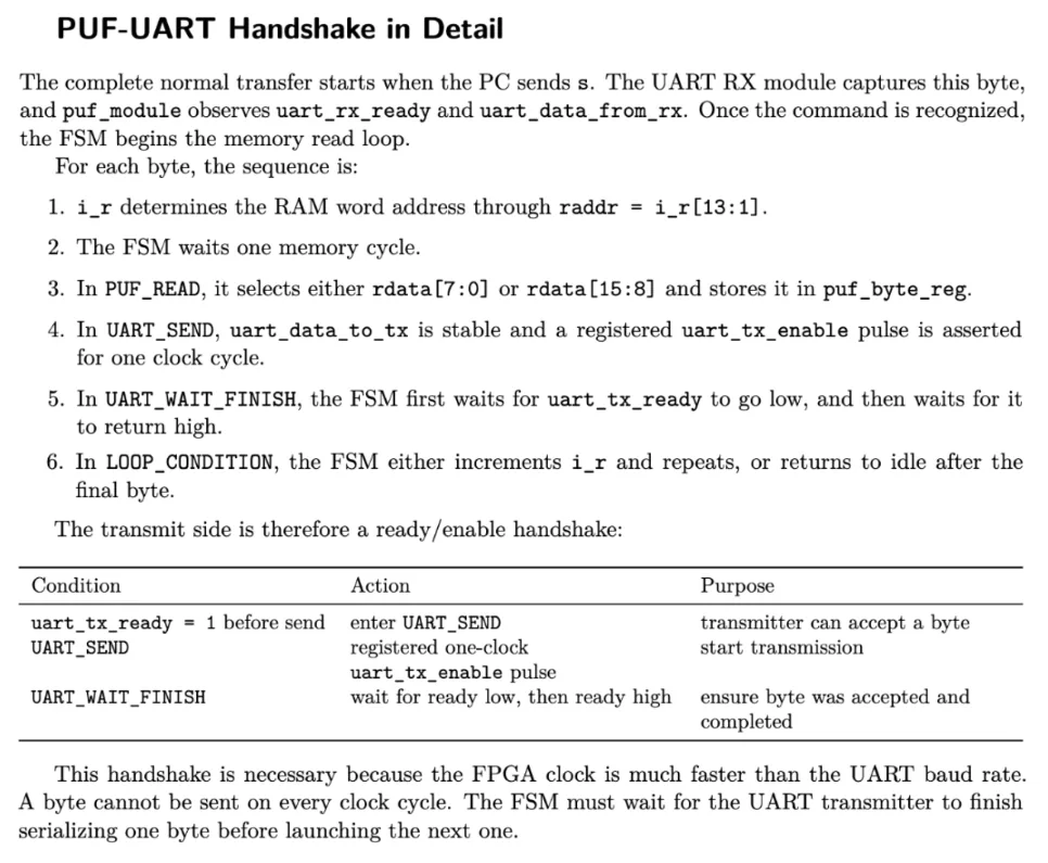
The UART module exposes a small ready/enable style interface. The PUF
controller presents one byte on uart_data_to_tx, then asserts
uart_tx_enable for one clock cycle when the transmitter is ready.
There is one timing trap in that interface: seeing
uart_tx_ready high does not necessarily mean that the byte you
just requested has already been transmitted. It may still be high from before
the transmission started.
During bring-up, the FSM treated this immediately-high ready signal as if the transfer had already completed. The result was that the same byte could be accepted twice, which showed up as paired bytes in the debug stream.
The fix was to make the transmit pulse registered and explicit, and then wait for the UART transmitter to actually become busy before accepting completion. The final sequence became:
- wait until
uart_tx_readyis high; - place the next byte on
uart_data_to_tx; - assert
uart_tx_enablefor exactly one clock; - enter a wait state;
- observe
uart_tx_readygoing low; - only then wait for
uart_tx_readyto return high; - increment the byte index and continue.
The uart_seen_busy register prevents the FSM from confusing
"the transmitter was already ready" with "the byte has finished
transmitting."
How the PC reads the response
The PC does not directly read individual PUF bits from the FPGA. It talks to the FPGA through a serial UART link.
The host script sends a one-byte command such as s for a normal
SRAM PUF readout or d for diagnostic mode. After receiving the
command, the FPGA starts streaming bytes back over UART.
The full readout is:
16 KiB = 16384 bytes = 131072 bitsOn the host side, the capture script collects these bytes and writes them as hexadecimal text. The final file shape is:
512 lines × 64 hex charactersEach line is then interpreted as one 256-bit response block. That format made the later analysis easier: the same bit position can be compared across repeated power cycles for reliability, while the bit distribution inside a response can be used for uniformity-style checks.
The capture script is therefore part of the measurement infrastructure. If it silently receives fewer bytes, repeats stale data, or writes malformed lines, the statistical analysis becomes meaningless.
From raw bytes to PUF metrics
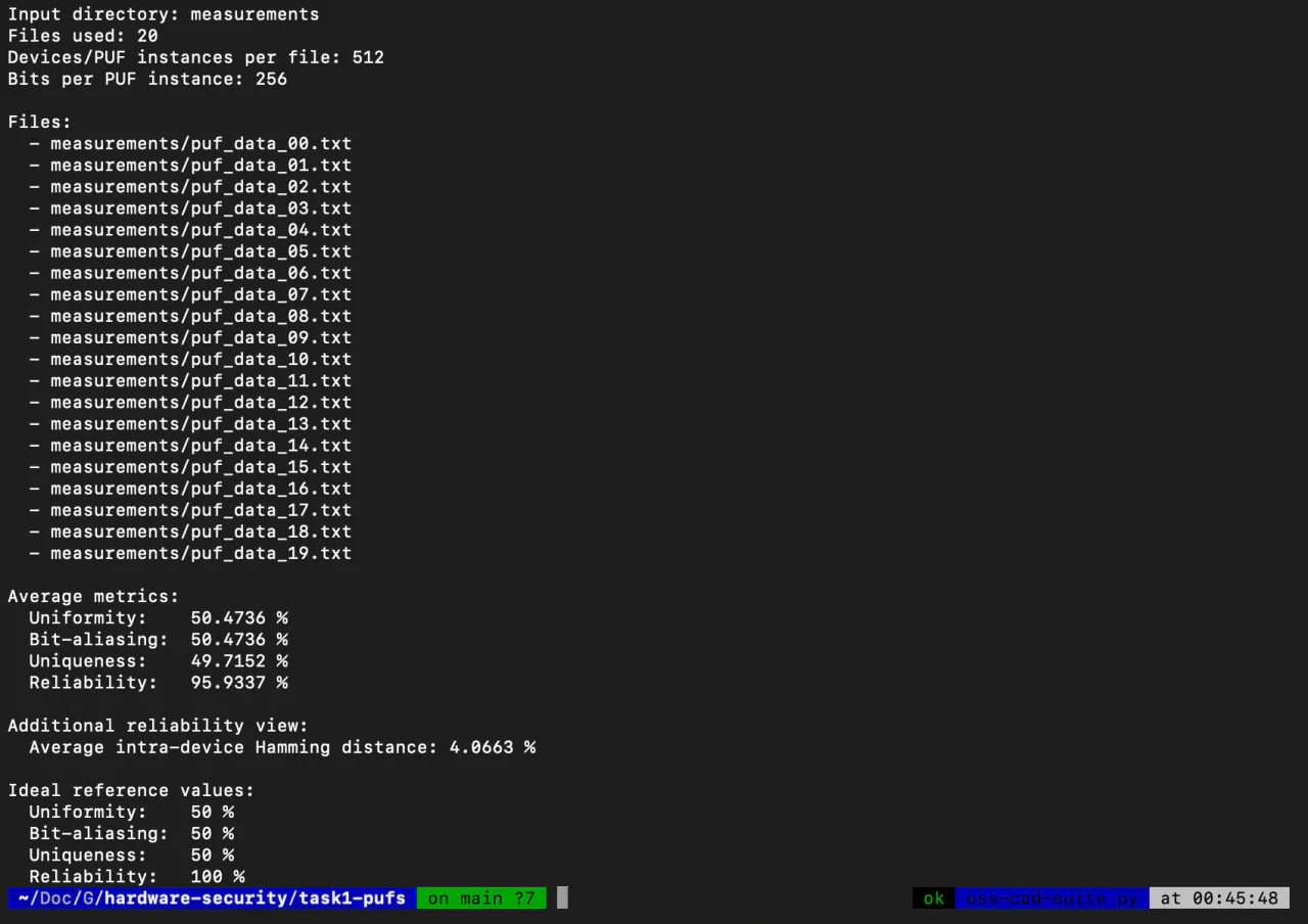
After the UART path started behaving, the task became more like a data analysis problem. The capture script produced hexadecimal readout files. I converted those hex strings back into bit vectors and then computed the first-order PUF metrics from those vectors.
Uniformity checks whether a response has a balanced number of zeros and ones. For each captured response, I counted the number of one bits and divided it by the response length. A perfectly balanced response would be close to 50%. If the value is far away from that, the memory startup pattern is biased toward either zero or one.
uniformity = number_of_ones / number_of_bitsBit-aliasing looks at the same idea from the bit-position side. For a given bit position, I checked how often that bit was one across multiple captured responses. If every bit position behaves independently and without global bias, these values should also be around 50% on average.
bit_aliasing[i] = number_of_responses_where_bit_i_is_1 / number_of_responsesReliability is about stability across repeated measurements. For this, I compared responses captured after repeated power cycles and counted how many bit positions changed. A reliable PUF response should not flip too much between repeated readouts of the same device.
The Python analysis was not complicated, but it only became meaningful after the FPGA readout path returned the expected diagnostic bytes every time.
Small Verilog lessons from this task
The Verilog part looked small, but it forced a few useful habits.
I made transmit pulses explicit. I cleared
uart_tx_enable by default on every clock and asserted it only in
the state that intentionally sends a byte. This avoids accidentally holding a
send request high for multiple cycles.
The byte index and RAM address are different concepts. The RAM returns 16-bit words, while UART sends 8-bit bytes. The controller therefore uses a byte index for the outgoing stream and derives the RAM word address from it:
raddr = i_r[13:1]The lowest bit selects which half of the 16-bit word is sent:
i_r[0] = 0  ->  rdata[7:0]
i_r[0] = 1 -> rdata[15:8]Debug output should not depend on the thing being debugged. The diagnostic stream was useful precisely because it bypassed the PUF data path and sent known constants. That made it possible to isolate the UART/FSM issue before trusting the SRAM readout.
Before measuring the physical effect, I needed enough independent checks to show that the pipeline was not inventing artifacts. The diagnostic stream provided that check for the UART and FSM path.
Measurements
Once the readout path became reliable, I collected repeated measurements and analysed the PUF response itself.
Where the effort went
In this task, hardware security depended more on bring-up and measurement engineering than I expected. Most of the effort went into digital design, UART communication, host-side capture, verification, and small debugging loops.
The PUF idea had to pass through a real hardware data path before it became a plot or metric. I could not separate the security claim from the measurement path that produced its data.
Next steps
I still need to analyse stability across resets and uniqueness across devices, if I can access more than one. I also do not yet know how much post-processing the response would need before it could serve as a reliable fingerprint.